- 您现在的位置:买卖IC网 > Sheet目录323 > DSP56311EVM (Freescale Semiconductor)KIT EVALUATION FOR DSP56311
�� �
�
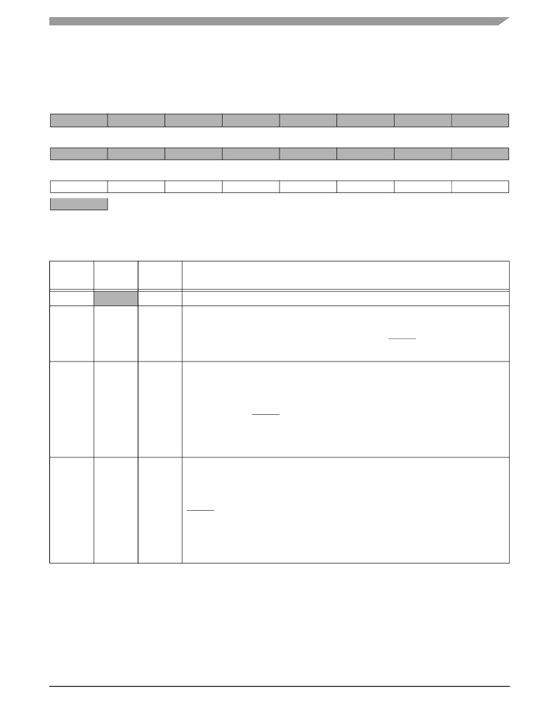
�SCI� Programming� Model�
�8.6.2� SCI� Status� Register� (SSR)�
�The� SSR� is� a� read-only� register� that� indicates� the� status� of� the� SCI.�
�23�
�15�
�7�
�R8�
�22�
�14�
�6�
�FE�
�21�
�13�
�5�
�PE�
�20�
�12�
�4�
�OR�
�19�
�11�
�3�
�IDLE�
�18�
�10�
�2�
�RDRF�
�17�
�9�
�1�
�TDRE�
�16�
�8�
�0�
�TRNE�
�—Reserved� bit;� read� as� 0;� write� to� 0� for� future� compatibility.�
�Table� 8-3.� SCI� Status� Register�
�Table� 8-4.� SCI� Status� Register� (SSR)� Bit� Definitions�
�Bit�
�Number�
�23–8�
�7�
�Bit�
�Name�
�R8�
�Reset�
�Value�
�0�
�0�
�Description�
�Reserved.� Write� to� 0� for� future� compatibility.�
�Received� Bit� 8�
�In� 11-bit� Asynchronous� Multidrop� mode,� the� R8� bit� indicates� whether� the� received� byte�
�is� an� address� or� data.� R8� is� set� for� addresses� and� is� cleared� for� data.� R8� is� not� affected�
�by� reads� of� the� SRX� or� SCI� status� register.� A� hardware� RESET� signal,� a� software�
�RESET� instruction,� an� SCI� individual� reset,� or� a� STOP� instruction� clears� R8.�
�6�
�FE�
�0�
�Framing� Error� Flag�
�In� Asynchronous� mode,� FE� is� set� when� no� stop� bit� is� detected� in� the� data� string�
�received.� FE� and� RDRE� are� set� simultaneously� when� the� received� word� is� transferred� to�
�the� SRX.� However,� the� FE� flag� inhibits� further� transfer� of� data� into� the� SRX� until� it� is�
�cleared.� FE� is� cleared� when� the� SCI� status� register� is� read� followed� by� a� read� of� the�
�SRX.� A� hardware� RESET� signal,� a� software� RESET� instruction,� an� SCI� individual� reset,�
�or� a� STOP� instruction� clears� FE.� In� 8-bit� Synchronous� mode,� FE� is� always� cleared.� If� the�
�byte� received� causes� both� framing� and� overrun� errors,� the� SCI� receiver� recognizes� only�
�the� overrun� error.�
�5�
�PE�
�0�
�Parity� Error�
�In� 11-bit� Asynchronous� modes,� PE� is� set� when� an� incorrect� parity� bit� is� detected� in� the�
�received� character.� PE� and� RDRF� are� set� simultaneously� when� the� received� word� is�
�transferred� to� the� SRX.� If� PE� is� set,� further� data� transfer� into� the� SRX� is� not� inhibited.� PE�
�is� cleared� when� the� SCI� status� register� is� read,� followed� by� a� read� of� SRX.� A� hardware�
�RESET� signal,� a� software� RESET� instruction,� an� SCI� individual� reset,� or� a� STOP�
�instruction� also� clears� PE.� In� 10-bit� Asynchronous� mode,� 11-bit� multidrop� mode,� and�
�8-bit� Synchronous� mode,� the� PE� bit� is� always� cleared� since� there� is� no� parity� bit� in� these�
�modes.� If� the� byte� received� causes� both� parity� and� overrun� errors,� the� SCI� receiver�
�recognizes� only� the� overrun� error.�
�DSP56311� User’s� Manual,� Rev.� 2�
�Freescale� Semiconductor�
�8-15�
�发布紧急采购,3分钟左右您将得到回复。
相关PDF资料
DSPAUDIOEVMMB1E
BOARD MOTHER DSP563XX
DSPIC30F2010 DEVELOPMENT KIT
KIT DEV EMBEDDED C
DSTRM-KT-0181A
DSTREAM DEBUG AND TRACE UNIT
DSUT1CSU
SURGE SUPPR NETWORK W/GROUND
DTEL2
SURGE SUPPRESSOR PHONE RJ11/RJ45
DV003001
PROGRAMMER PICSTART PLUS 16C/17C
DV164035
MPLAB ICD3 IN-CIRC DEBUGGER
DV164039
KIT DEV PIC24FJ256DA210
相关代理商/技术参数
DSP56311EVMIG_D
制造商:未知厂家 制造商全称:未知厂家 功能描述:DSP56311EVMIG DSP56311EVM Sample Code
DSP56311EVMUM
制造商:未知厂家 制造商全称:未知厂家 功能描述:DSP56311 Evaluation Module Hardware Reference Manual
DSP56311FACT
制造商:未知厂家 制造商全称:未知厂家 功能描述:DSP56311 Higher performance programmable DSP for demanding voice and data applications
DSP56311UM
制造商:未知厂家 制造商全称:未知厂家 功能描述:DSP56311 24-Bit Digital Signal Processor Users Manual
DSP56311UMAD
制造商:未知厂家 制造商全称:未知厂家 功能描述:DSP56311 Users Manual Addendum
DSP56311VF150
功能描述:数字信号处理器和控制器 - DSP, DSC 150Mhz/300MMACS 150Mhz EFCOP RoHS:否 制造商:Microchip Technology 核心:dsPIC 数据总线宽度:16 bit 程序存储器大小:16 KB 数据 RAM 大小:2 KB 最大时钟频率:40 MHz 可编程输入/输出端数量:35 定时器数量:3 设备每秒兆指令数:50 MIPs 工作电源电压:3.3 V 最大工作温度:+ 85 C 封装 / 箱体:TQFP-44 安装风格:SMD/SMT
DSP56311VF150B1
功能描述:数字信号处理器和控制器 - DSP, DSC 24 BIT DSP
RoHS:否 制造商:Microchip Technology 核心:dsPIC 数据总线宽度:16 bit 程序存储器大小:16 KB 数据 RAM 大小:2 KB 最大时钟频率:40 MHz 可编程输入/输出端数量:35 定时器数量:3 设备每秒兆指令数:50 MIPs 工作电源电压:3.3 V 最大工作温度:+ 85 C 封装 / 箱体:TQFP-44 安装风格:SMD/SMT
DSP56311VF150R2
功能描述:数字信号处理器和控制器 - DSP, DSC 24 BIT DSP RoHS:否 制造商:Microchip Technology 核心:dsPIC 数据总线宽度:16 bit 程序存储器大小:16 KB 数据 RAM 大小:2 KB 最大时钟频率:40 MHz 可编程输入/输出端数量:35 定时器数量:3 设备每秒兆指令数:50 MIPs 工作电源电压:3.3 V 最大工作温度:+ 85 C 封装 / 箱体:TQFP-44 安装风格:SMD/SMT